Biasing Of P-N Junction

Description:
Biasing in the process of applying potential difference to the semiconductor. Biasing is achieved by applying EMF across the P-N junction diode.
Biasing can be of two types –
- Forward biasing
- Reverse biasing
Forward biasing
When positive terminal of the battery is connected to P-side and negative terminal to N-side it is called forward biasing and the diode is said to be forward biased.
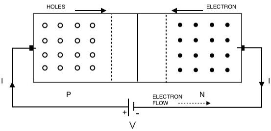
When forward biased, electrons from N-side and holes from P-side are pushed towards the junction.
The depletion layer’s width decreases.
As depletion layer decreases, potential barrier also decreases.
The potential difference within the P-N junction diode is known as induced potential (Vinduced) and potential difference applied externally is called applied potential (Vapplied).
Total Potential Difference = VInduced + VApplied
The direction of both the potential are opposite to each other therefore, as the applied potential increases it reduces the effect of induced potential.
When the applied potential is equal to the induced potential then, the net potential equals to zero and the depletion layer vanishes.
As there is no depletion layer, large number of electrons and holes cross the junction. They recombine and large current flows through the diode.
After recombining, the electrons travel as valence electrons then leave the Pregion and enter positive terminal of the source. A continuous current flows in the diode.
That is, on forward biasing, P-N junction diode acts as conductor.