Characteristic Of P-N Junction

Description:
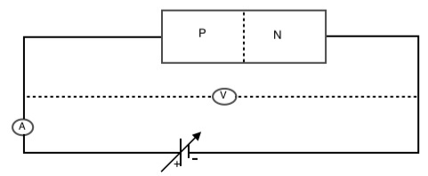
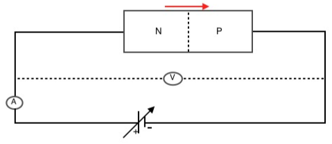
To study V-I characteristic of diode the external source is connected to diode through rheostat so that variable voltage can be applied to diode. A voltmeter is connected parallel to diode to read diode voltage and current meter is connected in series with diode to measure resulting current.
Characteristics can be studied separately for forward biasing and reverse biasing.
Forward characteristic
When forward biased (Si diode), initially current does not flow until biasing is less than potential barrier (0.7 V) but it increases suddenly beyond 0.7 V and current is directly proportional to voltage.
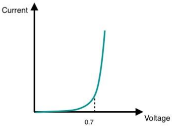
Resistance in forward biasing is dynamic resistance which is given by -
R = Δv/Δi
Resistance in forward biasing in the range of few ohm to ten kilo ohm.
Reverse characteristic
When the diode is reverse biased, there is no crossing of majority carriers and current is approximately zero.
A very small current of the order nA flows because of minority carriers in depletion region. This current is called reverse current.
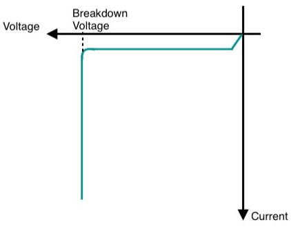
When reverse biasing increases, at a particular high value, the reverse current increases suddenly and a large amount of atoms are broken down in the depletion layer. This is called breakdown of diode.
If this reverse current is not controlled, p-n junction gets damaged due to excess heating. The reverse voltage, at which the diode breakdown occur is called breakdown voltage (VBR). For general purpose diode, the reverse voltage is always kept below the breakdown voltage.
Resistance in forward biasing is in the range of thousand kilo ohm.
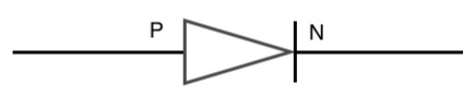
Symbol for P-N junction