P-N Junction (Diode)

Description:
When half part of a Si crystal is doped with trivalent impurity and half with pentavalent impurity, we get P-N junction diode.
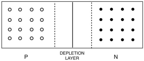
The border where p-region meets with n-region is called the junction.
P and N type junction develops a depletion-layer around it due to the recombination of electrons from N-side and holes on P-side.
No charge carriers are present in this region as combination of holes and electrons create neutral atoms, hence depletion-layer has high resistance.
No charge carriers from either side is allowed to cross the depletion layer.
Due to losing electrons ’N’ develops a positive charge layer, and ‘P’ develops a negative charge layer. Hence an electric field or potential difference is developed between the two.
This potential difference prevents the flow of majority charge carriers across the junction, hence called as potential barrier. When no external source is connected to diode it is said to be unbiased diode.
Majority charge carriers i.e. holes in the P side and electrons in the N side cannot flow through the depletion-layer, but minority charge carriers i.e. electrons in P side and holes in N side can flow through depletion-layer.
P-N junction diode acts as an insulator.