Reverse Biasing Of P-N Junction

Description:
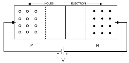
When positive terminal of the battery is connected to N-side and negative terminal to P-side, it is known as reverse biasing and the diode is said to be reversed biased.
In reverse biasing, free electrons and holes move away from the junction. Hence, increasing the width of depletion layer.
As the depletion layer increases, potential barrier also increases.
In reverse biasing the induced and applied potential are in the same direction i.e. the net potential will increase with the increasing applied potential.
Higher will be the net potential in the diode, higher will be the resistance.
Majority charge carriers cannot move across the junction, hence current will not be allowed to flow across the diode.
That is, on reverse biasing, P-N junction diode acts as insulator.
The current flowing in the reverse biased circuit due to the minority charge carrier is known as reverse current.